How to design a stackup for 4 layers PCB ?
When we are going to make a multilayer PCB, we need to consider the stackup design of the PCB. We should try to choose a stackup design that meets the requirements of use but can save costs if the PCB without special requirements of dielectric withstand voltage, impedance control and copper thickness, etc. .
The following are general designs for 4 layers PCB stackup of different thicknesses, which can be used as a reference:
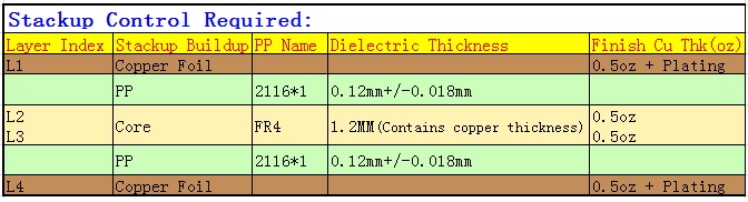
Finish Board Thickness 1.6mm+/-0.16mm :
Finish Board Thickness 1.2mm+/-0.12mm :
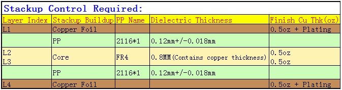
Finish Board Thickness 1.0mm+/-0.1mm :

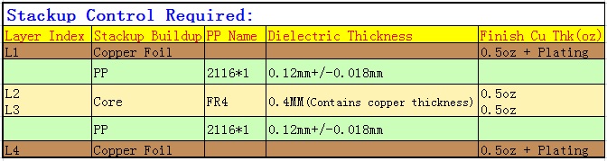
Finish Board Thickness 0.8mm+/-0.1mm :
【Print】
 Send Email
 Jeff
Jeff