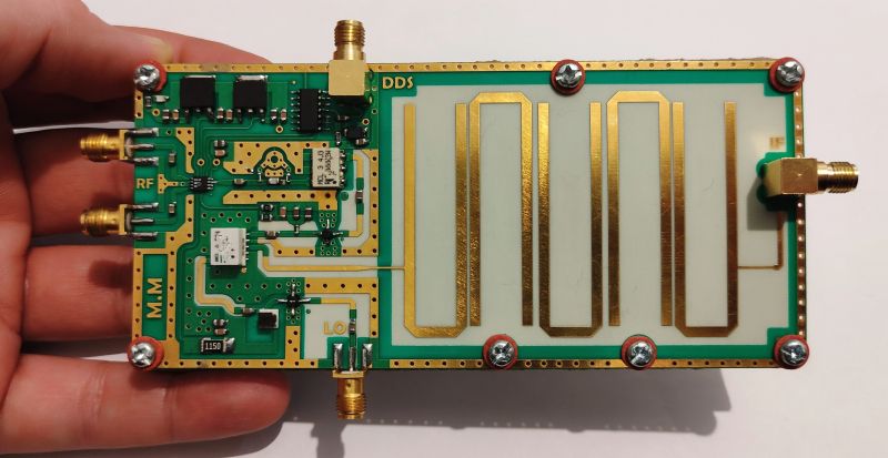
The art of RF & Microwave PCB design

The art of #RF and #microwave PCB design involves creating printed circuit boards (PCBs) that are optimized for #highfrequency applications.
RF and microwave #pcbdesign requires careful consideration of various factors to ensure optimal performance and #signalintegrity .
One crucial aspect is the layout of components and traces on the PCB. RF signals are sensitive to interference and #noise, so it's essential to minimize signal loss and maintain proper impedance matching. This involves placing components strategically, minimizing trace lengths, and using proper grounding techniques.
Another important consideration is the selection of materials. RF PCBs often use specialized materials with low dielectric constant and loss tangent to minimize signal loss and maintain signal integrity at high frequencies. These materials also help in reducing #electromagnetic interference (#EMI) and crosstalk.
RF PCB design also involves careful routing of #transmissionlines and impedance control. Transmission lines must be designed to match the characteristic impedance of the RF circuit to prevent signal reflections and maintain signal integrity. This requires precise trace widths, spacing, and controlled impedance routing techniques.
Additionally, RF PCB designers need to consider thermal management, as RF circuits can generate heat. Proper heat dissipation techniques, such as thermal vias and copper pours, should be implemented to prevent overheating and ensure reliable operation.
Simulation and testing are crucial in RF PCB design. Advanced simulation tools can help analyze signal integrity, impedance matching, and EMI issues before fabrication. Prototyping and testing the PCB with RF equipment can further validate its performance and make necessary adjustments.
Overall, the art of RF PCB design combines technical expertise, attention to detail, and an understanding of RF principles to create PCBs that deliver optimal performance in RF applications.