Multi-layer PCB differential impedance lines wiring experience sharing--From Shenzhen Vip Circuit Co., Ltd.

In our daily life, we are exposed to mobile phones, computers, and high-definition TVs every day. The core of them is PCB. In order to achieve high-speed data transmission, the production of printed circuit boards is inseparable from impedance matching.---Shenzhen Vip Circuit Co., Ltd. which is the professional PCB and PCBA manufacturer in China.
For example, the USB interface of a mobile phone can transmit two-way data synchronously, with fast speed and low cost. The two most common types are Type-A, Type-B, and Type-C.
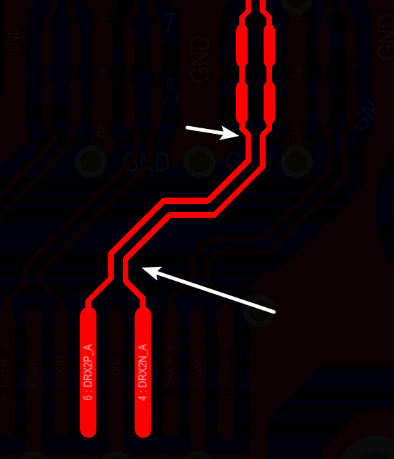
In the USB protocol definition (D+, D-), (TX+, TX-), (RX+, RX-) differential signal lines transmit digital signals. In order to ensure the stability of the transmission signal, it can effectively offset the common mode interference of the boundary and suppress EMI. The circuit board design impedance differential line must be laid out strictly in accordance with the wiring rules of the differential signal.
Shenzhen Vip Circuit Co., Ltd. summarizes the following points:
1. The components should be placed as close as possible during the layout, shorten the distance between the components to make the differential impedance line the shortest, and design as few vias as possible.
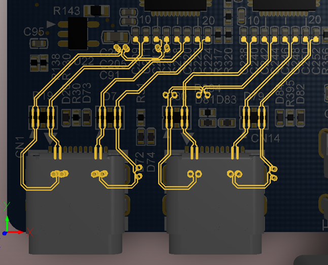
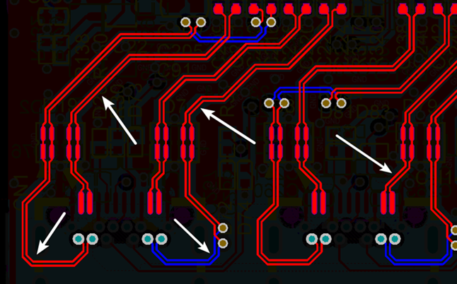
2. The routing of the differential impedance line must be parallel and symmetrical. The corner line cannot be run at 90°, and the routing should be designed at 45° or arc.
3. When connecting resistors and capacitors in series, the resistors or capacitors are designed to be aligned up and down or left and right.
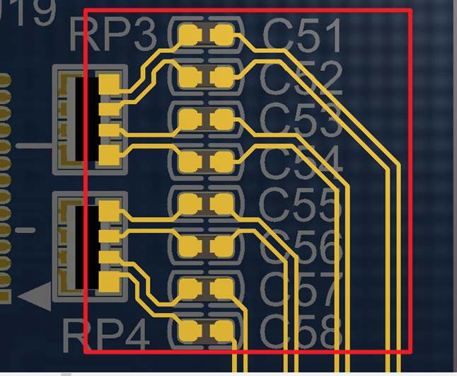
4. Try to design the differential impedance line to have the same line length and line spacing to avoid impedance deviation and common mode interference.
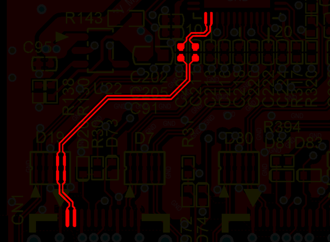
5. Due to the influence of component pin distribution, vias, and wiring space, the impedance differential line length does not match. Once the line length does not match, the timing will be shifted, and it will also cause common mode interference and reduce the transmission quality of the signal. .Therefore, it is necessary to compensate for the mismatch of impedance differential lines to match the line length and ensure that the length tolerance is within 5 mils.
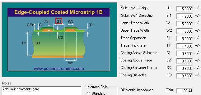
Shenzhen Vip Circuit Co., Ltd. uses Polar Si9000 to calculate impedance. The specific parameters are as follows:
H1: dielectric thickness (the thickness between the impedance line and the reference layer)
Er1: The dielectric constant of the PCB material, the value of FR4 is generally in the range of 4.0-4.6
W1: Design impedance line width
W2: upper line width = design line width minus 0.5mil
S1: the distance between the two impedance lines
T1: Copper thickness, 1oz is calculated according to the thickness of 1.4mil
C1: Thickness of solder mask oil on the substrate surface
C2: Thickness of solder mask oil on copper foil surface
C3: Thickness of solder mask oil between impedance lines
CEr: The dielectric constant of the solder mask oil 3.5
 Send Email
 Jeff
Jeff