What is Backdrilling in PCB Fabrication?

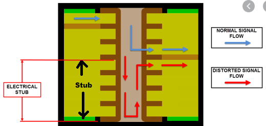
Back drilling or Controlled depth drilling is a process used to remove the unwanted portion of a PCB Via Stub. Plated Through Hole (PTH) Vias are used to connect two or more layers of a Printed Circuit Board to each other. However often, a via does not need to run the entire thickness of the board to connect each layer. For example, if we have a 10 layer PCB and need to connect layer 1 to layer 3 using a via, the PTH via runs through all the layers of the PCB even though layers 3 to 10 do not need to be connected to each other using that particular via. This unused portion of the via is called a stub. These stubs can cause significant signal distortion.
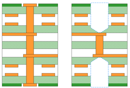
Backdrilling is a technique used to remove the unused portion of the stub (conductive plating) in a printed circuit board. This is removed by using a drill that has the diameter slightly larger than the diameter of the original via (PTH) hole. In practice, it is achieved by re-drilling the PTH down to a predetermined stub length of less than 10 mils from the signal layer.
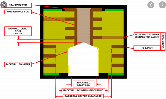
In case the via is connecting two internal layers only, then it is necessary to remove the top and bottom stub to improve the high-speed signal quality (see figure below). Backdrilling is a cost-effective solution as compared to the lamination technique (used for blind and buried vias) to manage the signal quality in a high-speed signal bath. If properly executed, it will not affect the performance and reliability of the PCB.
How does the stub length distort the signal quality?
When a signal flows down the length of a via, it splits into two parts at the junction between the internal layer and stub. One part travels towards the receiver end through the internal layer, and the other part travels towards the stub end. The stub act as an unterminated transmission line, so the signal reflects back towards the junction. At the junction, the signal again split into two with one signal returning to the source, and the other following the trace. Hence, the source signal is disturbed. The source distortion is the main cause for deterministic jitter (deviation clock pulse edge from its original position). Then the deterministic jitter leads to an increase in Bit error rates (BER), cross talk, EMI/EMC radiation, and the attenuation.
 Send Email
 Jeff
Jeff