A History of the Printed Circuit Board (PCB)
")
The printed circuit board (PCB) was created almost 100 years ago as an alternative to bulky wiring circuits. It is the heart of electronics today, supporting new designs like IoT and AI. This is a significant step forward in the evolution of the PCB, from a radio circuit with copper layers on each side of an insulation layer to multi-layer flexible PCBs used in satellite and defense applications.
The first printed circuit boards were built in the early twentieth century. They became more popular after Charles Ducas, an American inventor, created an electrical path through an insulated surface in 1925. This "Printed wire" method was also patentable by Ducas.
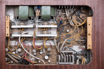
Paul Eisler, an Austrian engineer, made the first functioning PCB in 1943. It replaced the bulky wiring of a radio tube. The PCB design was created by etching a circuit onto a copper foil and bonding it to a non-conductive substrate. This technique produced reliable results. During World War II, the British and U.S. governments used PCBs to create proximity fuse circuits for bombs and artillery shells.
Electronics industry innovations during World War II led to significant advancements in PCB design.
The U.S. military increased the production of PCBs by using auto-assembly methods. Through-hole plating was used to create double-sided circuits. Copper-coated vias transmit electrical signals across the board. To prevent corrosion, zinc plates were also used in PCB design. The transistors further enhanced the PCB's functionality and reliability.
PCBs During the IC Era
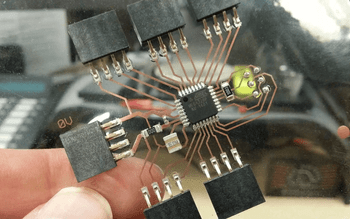
The 1960s saw the advent of integrated circuits (ICs), revolutionizing PCB design. A single chip could replace multiple parts. The conductor layers in PCB stack-up increased with the introduction of ICs. Multi-layer PCBs were possible because of this. Despite the reduction in circuit size, soldering connections became more difficult.
To simplify soldering, a solder mask was made of thin polymer material. This reduces the formation of bridges between adjacent pins and discrete components. The circuit was coated with a photo-sensitive polymer coating, dried, and then exposed to sunlight for imaging. This method was adopted as a standard in the PCB manufacturing process.
In the 1980s, surface-mount components were popular. Surface-mount technology (SMT) allowed for the automation of the assembly process. This greatly improved circuit performance and optimized power consumption. Manufacturing costs were also lower than the through-hole technique with SMT assembly.
SMT technology was crucial in automating the PCB assembly
In the 1980s, the designers created the circuits manually using stencils. With the advent of computers, electronic design automation (EDA) methods were introduced. Computer-aided design (CAD) was quickly adopted by PCB designers. This allowed them to quickly and efficiently draw complex circuits. To support small PCB productions, component manufacturers focused on making smaller components at lower prices.
PCBs in the 1990s and Beyond
The PCB applications' range grew as the PCBs' functionality, and density increased. The IC packaging technology ball grid array (BGA) was created in the 1990s. This package allowed the PCB functionality to be placed in the lower part of the component. Due to increased board complexity, design for testing (DFT) guidelines were also required. It was crucial to ensure that the PCB design was quality controlled. These developments led to a new era in the PCB manufacturing industry.
Design for testability or DFT manages major PCB considerations during the layout stage
With increasing circuit complexity, layout routing techniques became more complex. Micro vias were therefore introduced to high-density PCB design. Flexible PCBs were popular in applications that required a wide range of motion. The next step was every layer interconnection (ELIC), one of the most complicated types of high-density interconnect (HDI), PCBs. It was first developed in 2006 but was widely used only in the 2010s.
In the 2010s, a new generation of portable devices had extended capabilities. These devices, such as smartphones and tablets, commanded a significant market share. This was also the time when the automotive PCB market grew. One of the most significant changes in 2017 was the broader application of HDI PCBs' substrate material to import the system-in-package (SiP).
This chronicle shows how the PCB industry has made great strides. It starts with selecting a PCB substrate, applying a surface coating, drilling methods, and the overall fabrication process. Glass epoxy and phenolic papers were previously used. The end application will determine which substrate is best for you. PCB suppliers can provide a variety of substrates such as acrylic, epoxy adhesive, polyimide, and polyethylene terephthalate. High-speed applications will require rigid boards made from low-loss thermoset adhesives. Metal core substrates can be used for LED applications to provide heat dissipation.
The Future of PCBs
The consumer market has grown with the increasing demand for smartwatches and smartphones. Implantable devices and health monitoring are becoming more common every day. There are also safety devices such as fire alarms and CCTV that depend on small PCBs to function. Complex PCBs are used in advanced aerospace, telecommunications, and military applications for reliable and robust performance.
The PCB industry's electronic waste has raised environmental concerns. Bio-degradable substances are being evaluated as possible alternatives to hazardous substances. This is why technological innovations are crucial for PCBs and the rest of the electronics industry. This is an example of how developments in the automotive sector--electric cars and autonomous vehicles--are elevating PCB design to a new level.
The PCB industry has a history of innovations aligned with the more significant trends in the electronics industry
Virtual reality (VR) and augmented reality(AR) devices can influence the flexible PCB design. This allows electronic devices to be positioned in unusual shapes. In the future, PCBs may also be used as active components, which will reduce the number of elements in the circuit design. The latest 3D printed electronics can be made using an additive manufacturing process to construct a 3D PCB.
An overview of the history and evolution of PCBs shows how they have successfully adapted to emerging technologies. The turnkey assembly has sped up the process of PCB development. These advancements will continue to be made in the PCB industry.
 Send Email
 Jeff
Jeff