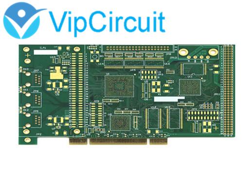
| Name: | Gold plated PCB |
|---|---|
| Surface treatment: | Gold Finger Plating |
| Finished copper thickness: | 1OZ |
| Material: | FR4 |
| Layer: | 4 |
| Finished board thickness: | 1.6mm |
| Min hole size: | 0.25mm |
| Solder mask color: | Green |
| Silkscreen color: | White |
Product Description
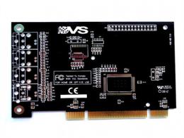
Multi-Layer rigid PCB,Connecting finger or gold finger plating with impedance control PCB design,in common use for mainboard, Graphics card, network card, memory card.
Standard gold finger:Gold fingers are of equal length.
Staged gold finger PCB:The etching pattern of the golden finger position needs to be realized by multiple film pasting, exposure and solder masking. The position and pattern need to be strictly and accurately controlled.
Long-short gold finger PCB:Its process is similar to the staged gold finger, which requires multiple exposure and electroplating to obtain the graphics of the long- short gold finger and requires the following design rules: plated holes, SMD and pads should not be placed within 1.0 millimeters of the gold finger; plated pads cannot exceed 40 millimeters in length.
As more and more technologies rely on gold fingers, it is vital that we have them plated and tested to meet the highest standard and to ensure the highest performance. Vip Circuit provides the PCB with the highest quality for customers from different industries with our extensive experience.


