What Are Microvias in PCB Design?

A printed circuit board (PCB) is the heart of electronic products. They provide the conductive pathway that allows all electronic components to function and connect. Multiple layers of PCBs are used to connect complex electronics.
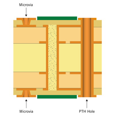
When copper is plated on the holes, holes are made through the PCB to route electrical connections between layers. These holes are known as vias (plated through-holes). The hole can be classified as a microvia, depending on its diameter.
What is a Microvia?
According to the Institute of Printed Circuit Boards, a microvia is any hole drilled in a PCB with a 1:1 aspect ratio and not exceeding 0.010 inches. The IPC used to consider microvias according to their size if they were smaller than 0.006 inches. With the advancement of technology, lasers can drill these small holes more often.
The IPC adopted the microvia definition of the 1:1 aspect ratio to prevent meanings from changing. Microvias, also known as uVias or microwires, can be used to connect layers within a PCB. They are usually limited to connecting two layers at a time.
The Different Types Of Microvias
PCB designers have many options for drilling microvias. Each microvia is the same in size. Their placement is the main difference.
Blind Microvias- Drilled to allow connections between the surface and an inner layer. These holes are not as deep as a through-hole but only reach one side of the PCB.
Buried microvias are holes in the inner layer of the PCB which do not reach the circuit board's surface.
Stacked microvia - several blind or buried microvia are stacked on top of each other to allow for the inner layers to be connected.
Staggered microvias are layers of multiple buried microvia. These microvia do not stack on top of one another. They are instead placed in an offset fashion.
Via In-Pad Microvias is a method of placing microvia holes directly onto the copper solder pad. This allows PCBs to become miniaturized.
Advantages Of Microvias In PCB Design
Microvias can be used for circuit board designs by PCB designers. Microvias provide thermo-mechanical reliability for the functions and performance. The ability to make via-in-pad microvias allows the board to be miniaturized. Because microvias are smaller than standard vias or plated through holes, they save space on circuit boards. You don't need to have bigger boards to accommodate all the components.
Microvias can be used to minimize defects in PCB designs. Lasers are used for drilling the holes. Because the trace lengths of microvias are shorter, there are fewer fabrication problems. Microvias have significant effects on signal integrity when creating an HDI circuit board. Higher radiation levels are created by using larger vias for high-speed circuits. Microvias can enhance RF capabilities and EMC characteristics. Microvias are more reliable than other types of vias and through holes.
Designing with microvias
There are many aspects to drilling microvias for PCBs. When designing circuit boards, you should ensure that the microvia does not exceed the 1:1 aspect ratio. Although it is possible to drill at a higher ratio, it won't be reliable and will most likely cause plating defects. Our PCB designers won't go below a 4-mil diameter, regardless of aspect ratio. The copper content of the PCB design must not exceed 1/2 oz when drilling into copper with a laser drill. The laser is more efficient at drilling holes and ablating the copper below the surface of copper, but the thickness of the copper will increase.
Each layer receiving a via must have an additional lamination step if it is to be placed in multiple layers. If you do not intend to use holes, they can be filled with a non-conductive material or plated closed. Microvias may not require filling because they are so small. The plating is done in copper, a special bath used to produce the chemistry. This process allows the fabricator to be more flexible in his design process.
Clearances will be required along the second pass-through layer if a layer is removed, such as blind microvias moving from one layer to another. If the second layer is needed to connect to the first layer, microvias that can be stacked or staggered may be used. Staggered vias, however, are simpler to make and offer greater reliability.
Conclusion
Because microvias allow PCB designers to be flexible in the fabrication process, customers can connect multiple layers with greater reliability. Microvia drilling is more compatible with some materials.
Talking with the PCB fabricator before selecting the material set will allow you to understand your options thoroughly. 911EDA engineers are skilled in helping customers choose the suitable materials for their application and connecting your electrical components. You may also be able to reduce material costs by using microvia drilling. Vias can reduce the size of your boards and save space. PCBs manufactured with low manufacturing defects and risk may offer significant cost savings.
 Send Email
 Jeff
Jeff