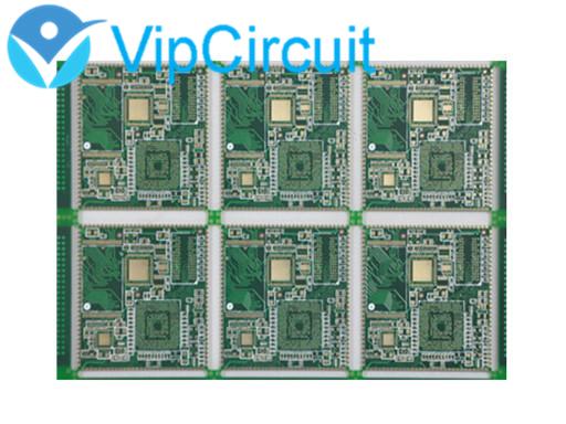
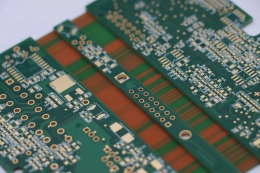
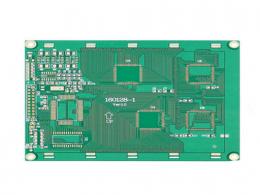
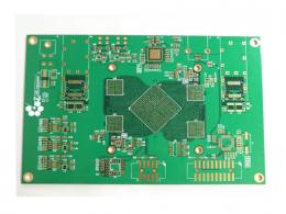
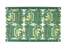
| Name: | Half PTH PCB |
|---|---|
| Surface finish: | ENIG,immersion Tin,silver, OSP, HASL, LF-HASL |
| Finished copper thickness: | 1OZ |
| Material: | FR4 |
| Layer: | 12L |
| finished board thickness: | 1.6mm |
| Min hole size: | 0.25mm |
| Solder mask color: | Green |
| Silkscreen color: | White |
Product Description
PCB with edge metallization & edge metallized half hole
Generally there are two methods to make metallized half hole for printed circuit board
1,Using pattern plating(alkaline etching) process,that is milling after pattern plated and plating Tin,utilize the alkaline etching liquid to remove the burrs,because at this time the burrs copper is exposured after milling,there is no tin protect.
2,Using metal hole masking (acid etching)process,that is before milling board,use second drilling to drill the hole wall which cross the profile,this step will avoid the milling cutter dragging the hole copper to appear burrs.
In terms of this kind of board,(half PTH hole/slot or lateral metallized), the process capability and engineering ability of the PCB manufacturers is very important.Some factories can hardly avoid this problem.(burrs in holes).
Please kindly send your files to us,you will get satisfactory results. Fast quote in 2 hours sales@vipcircuit.com
Technology Summary
| PCB Features | Ø PCB with up to 30 layers | Ø Impedance control |
| Ø Flex PCB up to 6 layers | Ø Via plugging/Laser hole stacking | |
| Ø Aluminum core | Ø Special material | |
| Ø Heavy copper(power boards) | Ø Hybrid (RO4350+FR4) | |
| Ø Blind and buried Vias | Ø Gold plated | |
| Ø HDI | Ø Min hole 0.2mm | |
| Ø RF(High frequency) | Ø Max copper thickness 6oz | |
| Surface Treatment | HASL/LF HASL | |
| ENIG/ENEPIG | ||
| Immersion Tin | ||
| Immersion Silver | ||
| OSP | ||
| Gold Finger/Gold plated | ||
| Selective Chem Au | ||
| Material | FR-4 |
CEM-1 |
| Halogen-free | PTFE | |
| Rogers | Polyimide | |
| Arlon | Hybrid | |
| Isola | BT | |
| High TG | Ceramic filled | |
