How to calculate PCB impedance ?

With the development of science and technology, electronic products continue to develop toward high-density, multi-functional, high-frequency and high-speed signal transmission. At present, the signal transmission frequency of the backbone network has reached 100Gbit/s, and the corresponding single-channel transmission rate is as high as 10Gbit. /s even reached 25Gbit/s, and the high-speed signal transmission has maintained a rapid development trend. The high-speed development of signal transmission makes signal integrity problems such as reflection and crosstalk more likely during signal transmission, and the faster the transmission rate, the greater the signal loss. How to reduce the loss of signal during transmission and ensure signal integrity which is a huge challenge in the development of high-speed PCB.
Impedance Definition:
The total resistance generated by an alternating current flowing through a known frequency is called impedance (Zo). For PCB, the impedance of a signal layer to its adjacent reference layer under high frequency signals.
1. Main types of PCB impedance:
(1) Single-ended impedance: In electronic information products such as computers and wireless communications, the energy transmitted in the PCB is a square wave signal (pulse pulse) composed of voltage and time. The resistance it encounters is called single-ended impedance.
(2) Differential impedance: Two identical signal waveforms with opposite polarity inputs at the driving end are respectively transmitted by two differential lines, and the two differential signals are subtracted at the receiving end. The differential impedance is the impedance Zdiff between the two wires.
(3) Odd mode impedance: the impedance of one line to ground in the two lines, the impedance values of the two lines are the same.
(4) Even mode impedance: Two identical signal waveforms with the same polarity at the driving end, and the impedance Zcom when the two wires are connected together.
(5) Common mode impedance: the impedance of the first line to ground in the two lines, the impedance values of the two lines are the same, usually larger than the odd mode impedance.
Among them, the Single-ended impedance and the differential impedance are commonly used impedances.
2. The main factors affecting impedance:
W1/S1: line width/line space, the line width increases, the impedance becomes smaller, and the line space increases, the impedance becomes larger;
H1: the thickness of the dielectric, the thickness increases, the impedance becomes larger;
T1: copper thickness, the copper thickness increases, the impedance becomes smaller;
C1, C2, C3: the thickness of the solder mask, the solder mask thickness increases, the impedance becomes smaller;
Er1: dielectric constant, the Er1 value increases, the impedance becomes smaller;
CEr: dielectric constant of solder mask, the CEr value increases, the impedance becomes smaller ;
How to calculate PCB impedance ?
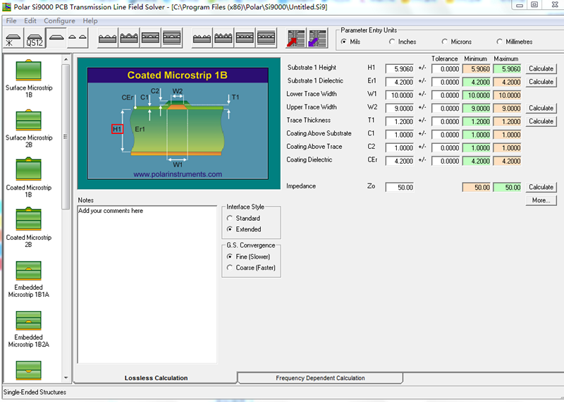
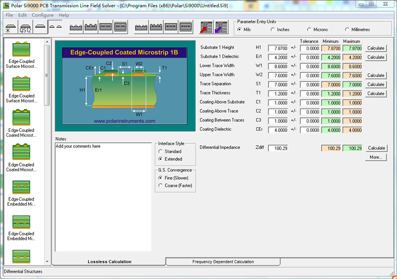
Nowadays, the most commonly used impedance calculation tool in the PCB industry is the Si9000 which is provided by Polar.
Firstly, you need to select the corresponding impedance model, and input the corresponding line width, line space, dielectric thickness, copper thickness, Er value and other related data, then you can calculate the impedance result.
Following picture for your reference:
Single-ended impedance:
Differential impedance:
 Send Email
 Jeff
Jeff